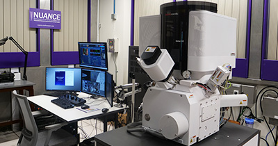
Features
SEM Column
- Resolution of 0.6 nm @ 2 –15 kV; <0.7 nm @ 1 k
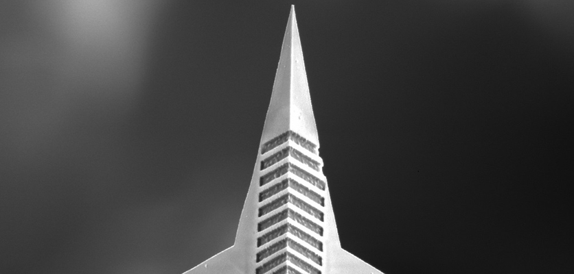
FIB Column
- 4 nm resolution @ 30 kV (Ga ions
Multiple Imaging Detector
- For secondary electron (SE), secondary ion (SI) and backscatter electron (BSE) imaging
- Retractable STEM detector
- Oxford large area (170 mm2) EDS detector
Deposition of carbon, platinum, and tungsten chemistries
- MultiChem Deposition System: Mixing gases and controlling flow rates to allow for multiple local gas chemistries
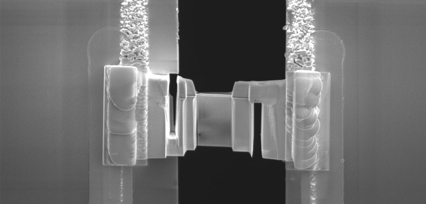
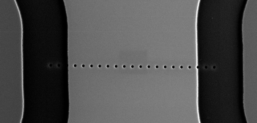
- Nanofabrication applications including (automated) TEM and atom probe tomography sample preparation
- Kleindiek Nanomanipulation system